

Request a Quote
Interested in more info and want to contact us?
Receive a FREE consultation within just 1 business day! We will answer all your questions and provide information on what you need!

-
Defect Detection: High-res lenses for particles, scratches, and pattern flaws
-
Dimensional Accuracy: Telecentric optics for line width and overlay measurement
-
Surface Profiling: Beam combiners for thickness and topography analysis
-
Spectral Tools: Optics for ellipsometry, Raman, and PL testing
-
Cleanroom Assemblies: Vibration-stable, contamination-controlled systems
-
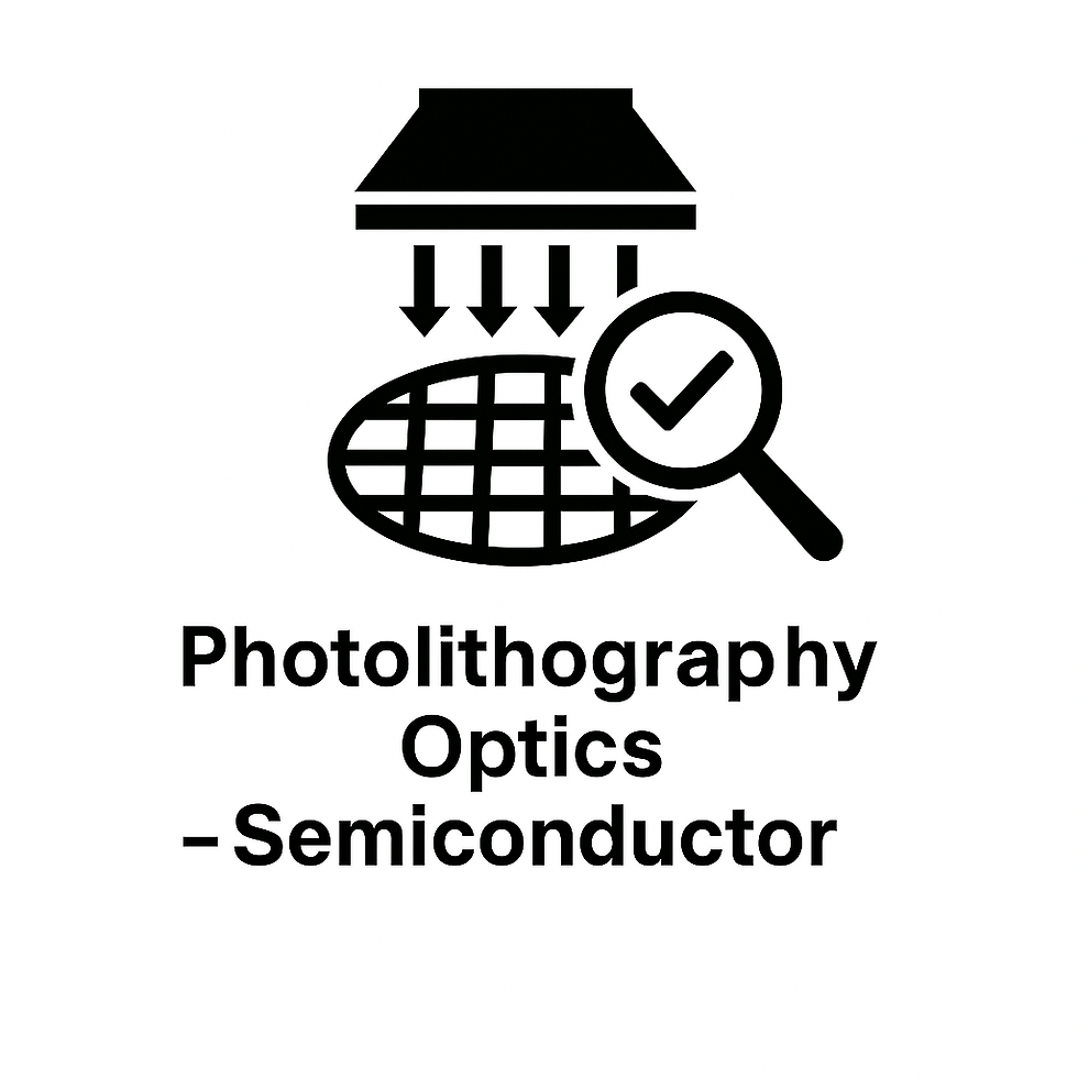
DUV Lenses: High-transmission optics for 193 nm lithography
-
Projection Systems: Catadioptric assemblies for sub-micron pattern transfer
-
Mask Illumination: Uniform beam shaping for consistent wafer exposure
-
Exposure Control: Optics for precise dose delivery and CD accuracy
-
Anti-Reflective Coatings: Thin films to reduce standing waves and enhance fidelity
-
Cleanroom Materials: UV-grade fused silica and CaF₂ for durability

- PL (Photoluminescence): Reveals bandgap, defects, and exciton behavior through emission analysis
- Ellipsometry: Measures thin-film thickness, refractive index, and uniformity with polarized light
- OES (Optical Emission): Monitors plasma processes in etching, deposition, and chamber cleaning
- UV-Vis & IR: Characterizes absorption, transmission, and reflectance across layers

-
Thin-Film Metrology: Ellipsometry and reflectometry for angstrom-level film and index measurements
-
Surface Uniformity: Interferometry detects flatness, roughness, and refractive index shifts
-
Defect Inspection: AOI optics identify particles, scratches, and pattern flaws in real time
-
Scatterometry (OCD): Measures nanoscale features beyond image-based techniques
-
Spectroscopic Testing: Raman and PL optics assess crystal quality and strain

Semiconductor Manufacturing
RMI delivers high-performance optics and coatings for semiconductor manufacturing, inspection, and metrology systems. From deep ultraviolet (DUV) lenses for photolithography to infrared components for thermal analysis, our custom solutions support critical processes across wafer fabrication and defect detection. With advanced thin-film coating capabilities and opto-mechanical integration, RMI enables OEMs to achieve tight tolerances, high damage thresholds, and spectral fidelity across UV, visible, and IR bands—driving innovation in microelectronics and nanofabrication.